
Digital-techniques-microprocessors


Basic Digital Techniques & Applications - PART 5
Combinational
Logic Circuits
Combinational Logic is a type of digital logic which
is implemented by Boolean circuits, where the output is a pure function of the
present input only.Hence it is also
known as time-independent / history-independent logic. We all know personal computer which we use
daily has Arithmetic and Logic Unit (ALU) for performing mathematical
calculations. This is also constructed using combinational logic circuits.
Examples of these circuits are
a) Half Adder
b) Full Adder
c) Half Subtractors
d) Full Substractors
e) Multiplexers
f) De-multiplexers
g) Encoder
h) Decoder
Let’s have a look at these examples.
a) Half Adder:
As the name indicates, it is used for addition of
numbers. The half adder adds two single binary digits A and B. It has two outputs,
sum (S) and carry (C).Since the circuit adds the two digits, it is called as
‘Half Adder’ circuit.

Truth
table of Half Adder circuit:

If we look at the truth table, for the first three
cases, the addition looks obvious. But for the last case, when A=1 and B=1 as
well, the sum =0 and carry is 1.
b) Full Adder:
The full adder adds the three one bit binary numbers
A, B and C and produces Sum and Carry as the output. The full adder is basically
a combination of adders.
Truth
table of Full Adder circuit:

If we see the first four records in this truth table,
it looks very similar to Half Adder circuit. The sum of row numbers 5,6,7 is
but obvious. For the last row,addition and carry is as shown below:
A=1
+ B=1
__________________
Sum=0 (Carry=1)
+C=1
__________________
Final Sum=1 (Carry=1) [See the final row]
K-map
simplification of Full Adder circuit:

Let’s have a look at the K-map simplification of Full
Adder circuit. Input variables are mentioned on the top left. Their possible combinations
for input digits 0 and 1 form a K-map. Please note the position of input
combination 10 and 11. This is all about positioning. The output ‘sum’ and
‘carry’ is mentioned inside the K-map.
Now, based on ‘true’ values of output, a quad (a group
of 4 logical high digits), pair (a group of 2 logical high digits) or singles
(a single digit) are formed.As shown in above diagram, for carry, 3 pairs are
formed. While for Sum, four singles are formed. Priority is always given to
quads and pairs as compared to singles.
The Logical expression is formed based on these quads,
pairs and singles. The expression is in SOP form, for ‘Sum’ K-map, the single
formed when A=1 and B=C=0 yields A . For digit
0, complement is written.
. For digit
0, complement is written.
Logic
Diagram of Full Adder circuit:
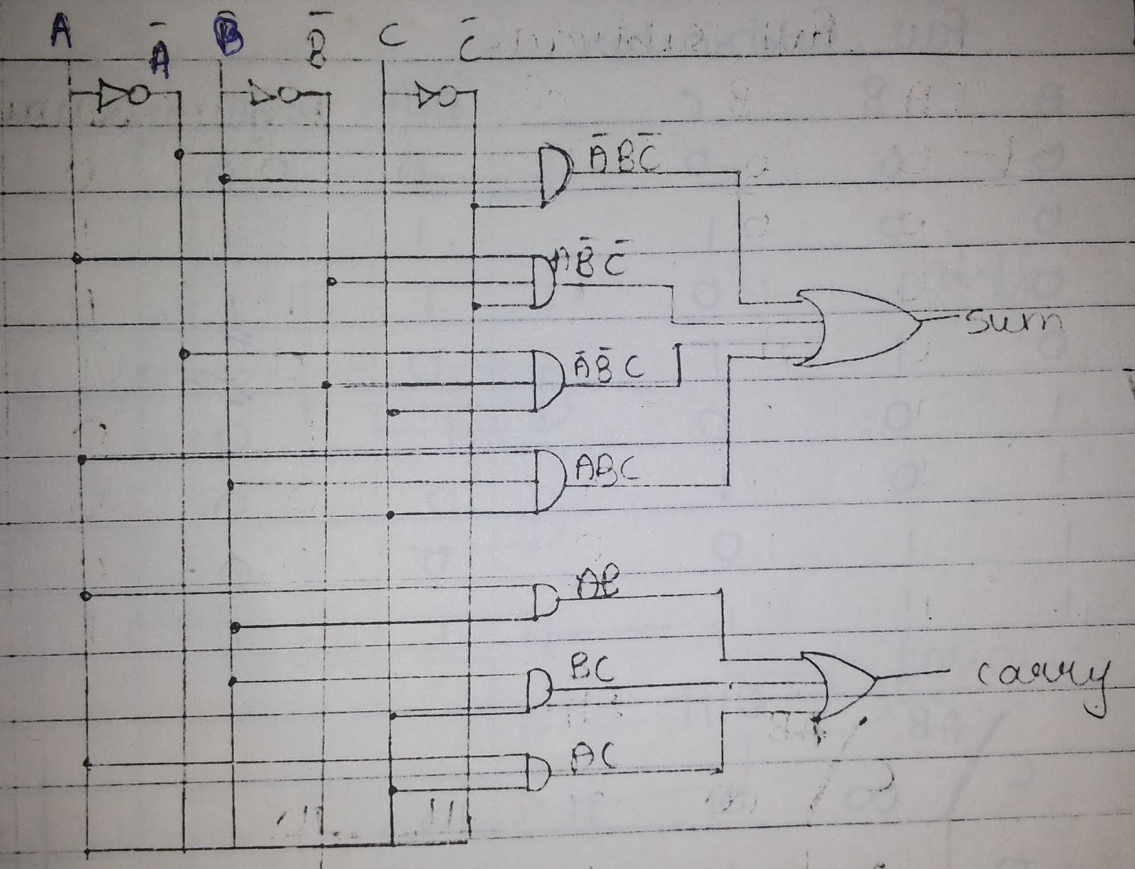
As shown in the diagram above, all the products are formed
with logical AND gate. For sum, logical OR gate is used.


0 comments:
Post a Comment